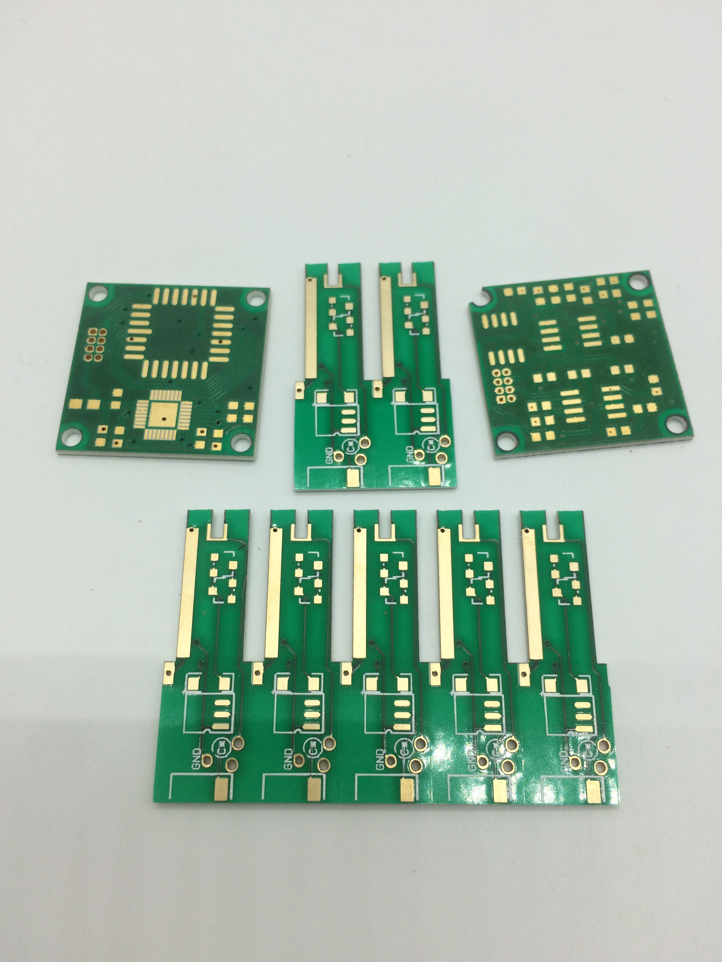

Ceramic PCB
When you are looking for substrates for electronic circuits with a high thermal conductivity and a low expansion coefficient (CTE), ceramic PCB will be your preferred choice of material. Today ceramics are already widely used as substrates in many microelectronic components and power LED packages and more and more they are replacing entire printed circuit boards reducing complexity in design and manufacturing while increasing performance. Examples are Chip-on-board (COB) modules, High power circuits, proximity sensors, battery drivers for EVs, …
Ceramics advantages over other printed circuit boards:
² Higher operating temperature up to 350ºC
² Lower expansion coefficient
² Good thermal properties
² Superior high-frequency performance
² Lower system cost: reduces test, insertion, assembly
² Smaller package size due to integration
² Cost effective for dense package due to parallel processing of layers
² Hermetic packages possible, 0% water absorption
KLS Company specializes in Alumina Oxide (Al2O3) and Aluminum nitride boards (AIN) for both thick film as well as Low-temperature Co-fired Ceramics (LTCC).
Alumina (Al2O3) is widely used because of its low cost. It is, however, a less good thermal conductor (24-28 W/mK) but still outperforms most IMS (metal core) PCB since it does not require a dielectric layer between circuits and core. If needed, thermal performance can be still enhanced using silver (Ag) filled vias. Boards are usually thicker (0.5mm-1.5mm).
Aluminum Nitride (AIN) has far better thermal performance (> 150 W/mK) but is also more expensive. Also here thermal performance can be further improved by Ag or Au traces and vias.
To maximally guarantee thermal performance and an optimal electric conductivity while reducing corrosion, KLS Company only uses Silver (Ag – 406 W/mK) for printing traces after which they will be covered with glass for protection. For high sulfur environments where silver corrosion can be an issue, we offer Gold plating as a solution to protect the exposed pads. Traditional PCB surface finishes like OSP or HASL cannot be used due to high sintering and operational temperatures.
Technical Specifications
|
Substrate Material |
Alumina Oxide - Al2O3 (96% or 99%) |
Alumina Nitride - AlN |
|
Category |
Thick film, LTCC |
Thick film |
|
Conductor material |
|
Silver(Ag)/ PdAg |
|
Masking |
Transparent glass coating, Black glass coating, High reflective coating |
Transparent glass coating, Black glass coating, High reflective coating |
|
Finish |
None(Silver Ag) or NiAu(Gold plating) |
None(Silver Ag) or NiAu(Gold plating) |
|
Max Layers |
10 |
10 |
|
Substrate Color |
White, Black |
Grey |
|
Panel size |
120mmx120mm standard (Max 180mmx180mm possible) |
110mmx110mm |
|
Panel size tolerance |
±50um |
±50um |
|
Thickness per layer |
0.1, 0.25, 0.38, 0.5, 0.635, 0.8 or 1.0mm |
0.25, 0.36 or 0.5mm |
|
Thickness tolerance |
±5�� |
±5�� |
|
Warpage (non-flatness) |
�Q±0.2�� |
�Q±0.2�� |
Frequently Asked Questions(FAQ)
Why do you claim ceramic PCBs in Alumina Oxide (Al2O3) have a good thermal conductivity compared metal core PCB (IMS) when you know Al (160 W/mK) and Cu (>200 W/mK) have a much higher thermal conductivity compared to Al2O3 (22 W/mK)?
Al & Cu have indeed high thermal performances but the dielectric layer which separates the metal core from the conductive traces will increase the thermal resistance significantly. Both the dielectric by itself (usually <3 W/mK thermal conductivity) as the interface resistance will reduce the total thermal performance. Depending on the thickness of this layer (<10 W/mK) the thermal conductivity of the board can be reduced by 70-90%!
Alumina (Al2O3), on the other hand, is a dielectric material and thus traces can be placed directly onto the board eliminating any loss in conductivity. Additionally, Elite Advanced Technologies is using Silver (Ag) (400 W/MK) metallization allowing the heat to spread even better over a large ceramic surface away from the sensitive component.
Ø Q1: Are ceramic PCBs expensive?
While ceramic boards are usually more expensive then FR4 & CEM3 boards, the cost of thick film Al2O3 is in line with Al metal core PCBs and even below Cu metal core PCBs.
Ø Q2:Can ceramic PCBs pass reflow and be used in SMT & pick-and-place machines?
Yes, both are possible.
Ø Q3:Can ceramic PCBs be multi-layer?
Yes and we have experience in making ceramic circuits up to 10 layers
Ø Q4:How big can ceramic boards be?
Our maximum standard size is 125mmx125mm or 5″x 5″ panels. Upon request, we can accommodate boards up to 180mm x 180mm (7″x 7″) or even larger.
Ø Q5:Is there also a solder mask layer and silkscreen possible?
Yes, we can add a protective solder mask layer in a glass which can be transparent or black. Also, silkscreen is possible.
Ø Q6:What should I take into account when designing circuits layouts for a ceramic board? What are your design rules?
You can download and see our complete design rules here.
Ø Q7:What is the difference between Thick film ceramics and LTCC?
Thick film ceramic boards are post fired which means vias, traces, stacking, etc… are only done after the board has been ‘baked’ already and is in its sturdy and hard form. On the other hand, LTCC or Low-Temperature Co-fired Ceramics are still in a relatively soft state when cavities, vias & holes are punched and traces are printed. This way, it is still possible to smooth & round inclinations so multi-shape and angled designs are possible. Only after this process, the board will be co-fired at a temperature of 900°C.
Product show